Solving EMC problems – a practical example
In a project, the interference emission of a device should be investigated before the EMC test is carried out by the TÜV.
This was a battery-operated medical device (DUT) with an applied part, which is powered by the DUT and communicates via UART.
The emission measurements were conducted in an EMC chamber with the antenna positioned 3 meters from the device. The antenna was aligned horizontally and vertically.
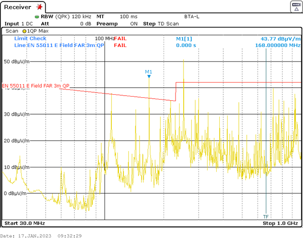
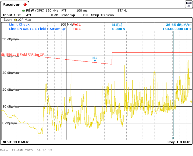
However, it became apparent that the device would not pass the EMC test as it was, as the limit was significantly exceeded in some places, while the peaks were only slightly below it in others. Incidentally, the limit values displayed are the standard settings of the measuring receiver. For us, the limit values for medical devices according to EN 60601-1-2 apply, which are similar but slightly different.
By the way, the limit values of the boundary line are not relevant for us, but are converted to the 3m antenna distance.
This article will discuss how to identify and minimize sources of interference that cause these peaks.
The images in the following chapters were taken with the antenna horizontal, as this is where the radiation was greatest.
Fundamental considerations
The first step should be to examine the peaks more closely and compare them with the frequencies used in the device.
| Frequencies with high peak values in emission measurements | ||||||
| 115 MHz | 144 MHz | 168 MHz | 192 MHz | 214 MHz | 220 MHz | 233 MHz |
| 240 MHz | 252 MHz | 288 MHz | 300 MHz | 336 MHz | 480 MHz | 504 MHz |
| 624 MHz | 720 MHz | 768 MHz | 816 MHz | 864 MHz | 912 MHz | 924 MHz |
For example, you can search for the following frequencies:
- Operating frequency of a switching regulator
- Operating frequency of a microcontroller
- Clock frequency of a communication interface
- Multiples of a used frequency
The device uses an EMMC and SDRAM as memory modules. Looking at the clock frequencies used by the memory and the peaks in the measurements, you'll notice some overlap (highlighted in color).
| Fundamental frequency and multiples of EMMC communication | ||||||
| 48 MHz | 96 MHz | 144 MHz | 192 MHz | 240 MHz | 288 MHz | 336 MHz |
| 384 MHz | 432 MHz | 480 MHz | 528 MHz | 576 MHz | 624 MHz | 672 MHz |
| 720 MHz | 768 MHz | 816 MHz | 864 MHz | 912 MHz | 960 MHz | |
| Base frequency and multiples of SDRAM communication | ||||||
| 84 MHz | 168 MHz | 252 MHz | 336 MHz | 420 MHz | 504 MHz | 588 MHz |
| 672 MHz | 756 MHz | 840 MHz | 924 MHz | |||
To confirm the suspicion that the problem is related to the memory chips, you can examine the device's electronics with a spectrum analyzer. This also offers the opportunity to locate possible sources of interference.
Spectrum Analyzer
A spectrum analyzer is used to search for sources of interference at the component level. Near-field probes are used to first examine the applied part's wiring, the wires within the device, and the display connector. The peaks from the laboratory tests could not be found here.
In the next step, the probes are used to search the entire circuit board for the frequencies that were critical in the preliminary test.
Tip: Start with areas where potential sources of interference are located, such as switching regulators or microcontrollers.
The power supply is unremarkable here, but two areas on the microcontroller stand out, showing many of the peaks from the preliminary test. You probably already guessed: these are the pins of the communication interfaces to the eMMC and SDRAM.
At this point, it's worth taking a look at the circuit board layout, as you can narrow down the area quite well. A closer look at the interface between the microcontroller and memory reveals that the layout isn't optimal.
There are cables that lead to connectors and are therefore open, the high-frequency cables are sometimes very long, the ground planes are not closed or are poorly connected and the UART cables to the application part are not sufficiently shielded from the high-frequency clock lines of the memory.
Minimizing interference emissions
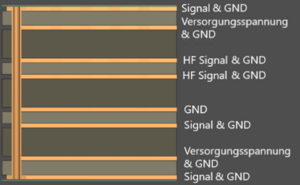
First, some theory about high-frequency lines…
The layered structure of the circuit board is shown here. The supply voltages are not continuous areas, but rather "islands" within a GND area. This is critical because the current path for the high-frequency signals cannot be optimally routed.
Unlike supply voltages and low-frequency signals, which choose the shortest return current path due to the lowest resistance, the return current path for high-frequency signals tries to follow the same path as the signal path.
If the return current path is not parallel to the signal path because it is interrupted by surfaces, both paths form a large loop. This loop can act as an antenna and lead to EMC problems.
To avoid such problems, free areas should be filled with GND and supply voltages should be routed as a printed circuit board. Furthermore, high-frequency lines should always be kept as short as possible.
With this knowledge, various measures can now be tested to minimize the disruption. Here are the measures implemented in this case:
- Shielding critical areas / components
- Capacitors on critical lines
- Adjusting the layout
Tip: Never test multiple measures at once to save time, as this will make it impossible to determine the actual cause of the problem. Testing the troubleshooting measures
First, the memory modules are shielded with copper foil and the measurements are repeated.
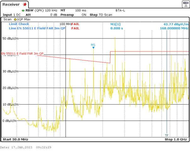
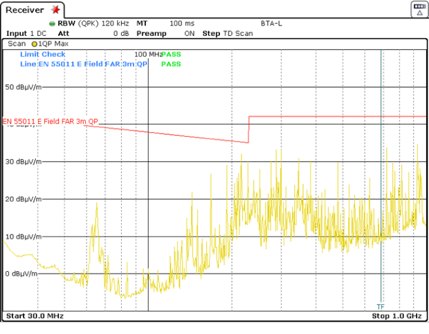
It can be observed that the peaks all fall below the limit.
The copper foil is then removed and a capacitor is placed on the UART line against GND close to the microcontroller.
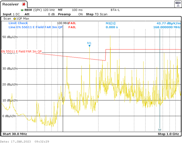
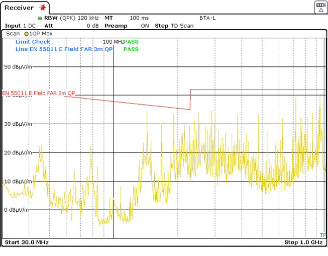
Here too, it can be observed that the peaks fall below the limit value.
This requires a layout change before proceeding with the EMC test. Here's a comparison of the EMI emissions measured at the SDRAM interface.
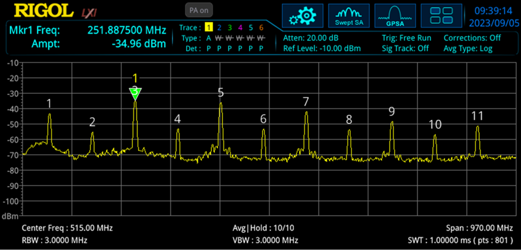
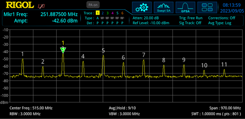
| Peak [MHz] | 84 | 168 | 252 | 336 | 420 | 504 | 588 | 673 | 756 | 841 | 924 |
| Alt [dBm] | -43,1 | -55,3 | -35,9 | -53 | -36,1 | -53,1 | -41,8 | -53,5 | -48,3 | -56,9 | -51,1 |
| New [dBm] | -49,8 | -60,4 | -42,6 | -53,2 | -45,1 | -54,9 | -51,3 | -58,6 | -57,9 | -65,4 | -64,4 |
| ∆ | 6,7 | 5,1 | 6,7 | 0,2 | 9 | 1,8 | 9,5 | 5,1 | 9,6 | 8,5 | 13,3 |
You can see that the peaks are lower at all frequencies, in some cases significantly lower than the previous values. With the new layout and capacitor on the UART line, we then proceeded to the EMC test.
Result of the EMC measurement
Despite modifications, the EMC laboratory initially shows the following result:
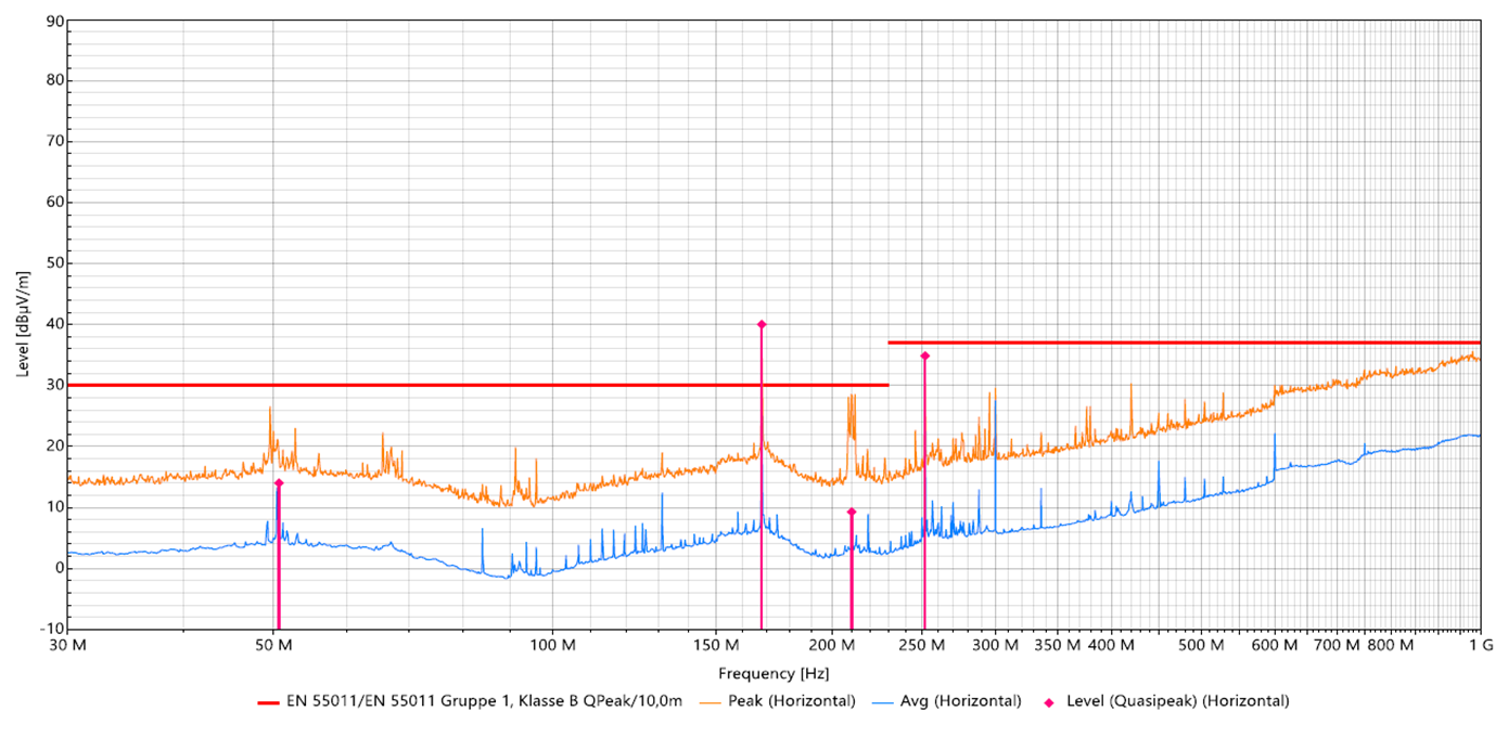
At 168 MHz, the peak is above the limit; if the applied part is removed, the peaks also fall below the limit. Since we know the frequency and the possible cause, there is a quick solution to the problem. A second capacitor is placed on the UART line, this time as close to the connector as possible. And after this modification, the repeat measurement looks like this:
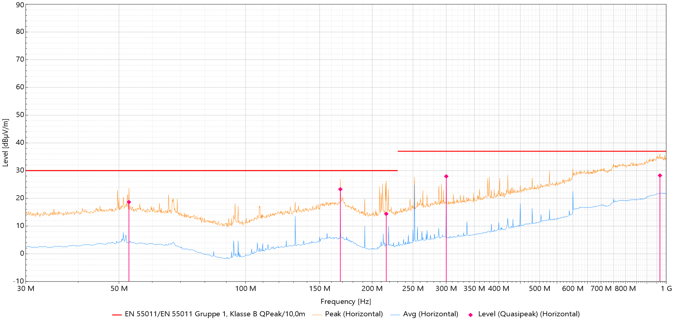
I hope you enjoyed the article. As you can see, sometimes a capacitor in the right place can be the solution to an EMC problem—of course, in conjunction with an EMC-compliant layout. If you need our support, e.g., through reviews or measurements, please contact us at any time.
